Single Nanowire Conductivity and Photoconductivity
For a number of years (eight to be exact) we, like others, realized that semiconducting nanowires coated with plasmonic nanoparticles, namely Ag and Au, will exhibit unique photonic characteristics. The motivation was our earlier work on sensors constructed with Au nanoparticle decorated GaN nanowires, where the sensors consisted of mats of nanowires. Au decorated GaN nanowires are complicated materials to fully understand due to the rich mixture of physics they embrace. First we have the plasmonic characteristics of the nanoparticles, which are not identical in size and therefore cannot produce a narrow plasmon band. On top of that one must account for the depletion layer which forms at the nanoparticle-nanowire interface. In addition, there is the question of how the surface plasmon polaritons of the discontinuous film scatter and how this energy is funnelled to the conduction electrons of the nanowire. Lastly, there is the waveguide properties of the nanowires, which depends on the diameter and length of the nanowire. This work is published in Nano Letters.
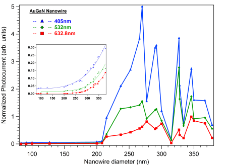
Above is the observed photoconductivity of bare and Au nanoparticle decorated GaN nanowires as function of diameter at different wavelengths. Note the oscillations of the normalized photocurrent of Au nanoparticle decorated GaN nanowires as a function of diameter, which is not observed for bare GaN nanowires. Also, the photocurrent of the Au decorated nanwires is greater than the corresponding dark current by as much as 500%, as compared to 30% for bare nanowires.
This diameter dependent oscillitory behavior is attributed to the allowable TM modes of the GaN nanowires and the width of the depletion layer at the Au-GaN interface. The image below are some of the allowable TM modes of a 400 nm diameter superimposed with the spatial dimensions of the nanowire and the depletion layer. As expected, the nanowires will be single mode waveguides and only if this mode lies in the undepleted region of the nanowire will the large enhancement of the photocurrent be observed.

